
Gate-Tunable XSTM
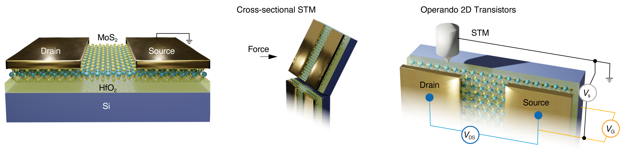
Gate-Tunable XSTM combines cross-sectional scanning tunnelling microscopy and spectroscopy with in situ gate and source–drain bias control. By probing a cleaved transistor in ultrahigh vacuum, it maps local electronic states and band-edge shifts across buried contacts and channels under operating conditions, revealing how electrical bias governs carrier injection.
Related publication · Nature (2026)
Using this approach, our team directly measured a carrier transfer length of approximately 2 nm in a bismuth-contacted monolayer MoS2 transistor, providing an experimental basis for assessing contact scaling in future 2D electronics.
Directly probing the carrier transfer length in 2D-material transistors
Zi-Liang Yang, Bo-Chao Huang, et al.
Nature 655, 350–356 (2026).
DOI: 10.1038/s41586-026-10707-0
Interface Science by Cross-sectional Scanning Tunneling Microscopy
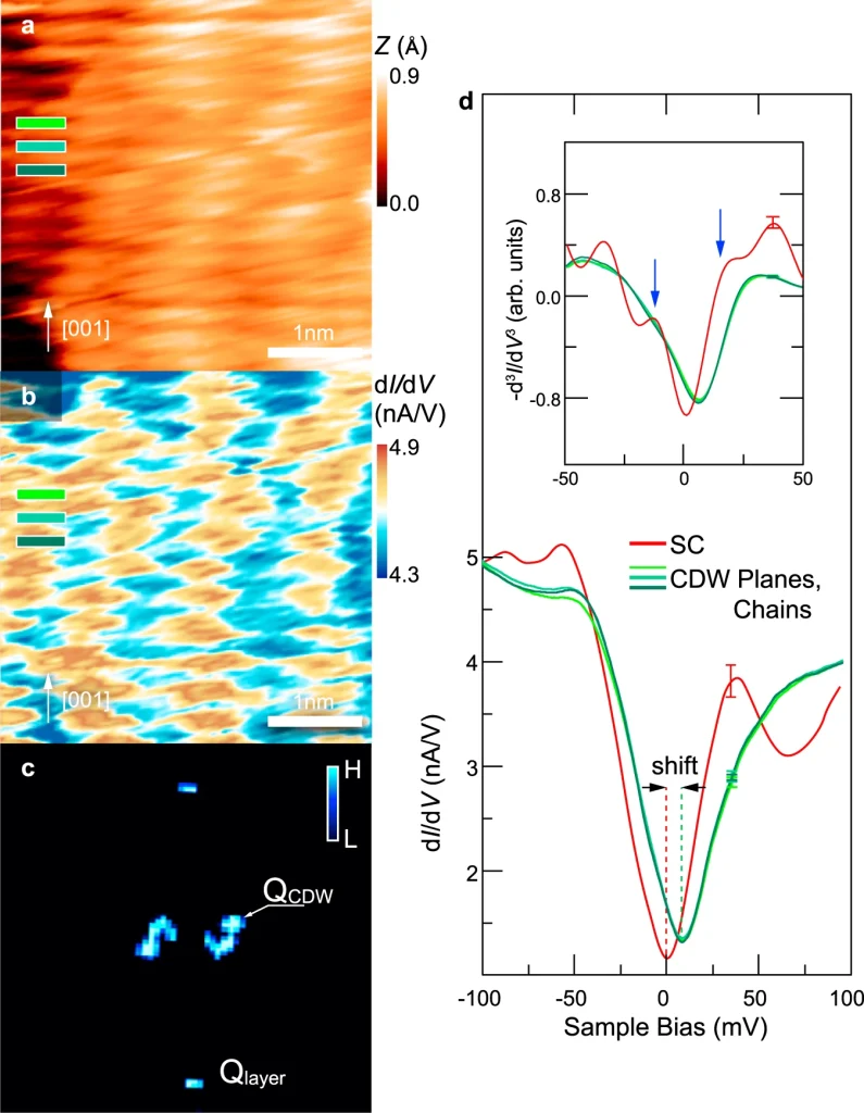
Scanning tunneling microscopy(STM), is a powerful tool to probing the electronic structure of materials in atomic scale. In our lab, we use STM to measure the materials heterostructure, such as complex oxides system, superconductors, photovoltaics, and electronic device. In this way, the band alignment and interface property like 2D electron gas can be directly measure and analysis.
Selected Publications:
Low-dimensional Materials Electronic Structure
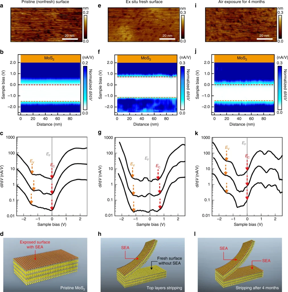
Low-dimensional materials is a group of materials with the size in nanometer scale, and can be classified into 2D, 1D and 0D materials. When things go down to low-dimension, the physics phenomena become very fascinating and the mechanism behind them still need to be investigated. STM allows for the creation of high-resolution maps of the local density of electronic states (LDOS) on the surface of a material, which can provide detailed information about the electronic structure at the atomic scale. This can be particularly useful for studying the electronic properties of low-dimensional materials, such as 2D materials and nanostructures, which have unique and often unusual electronic properties due to their reduced dimensionality.
Selected Publications:
Light-modulation STM for Optoelectronic Materials
For semiconductors, lights can excite the carriers from valence band to conduction band, and sometimes, it can even change the electronic structure or the lattice structure. In our group, we use LM-STM to study the optoeletronic materials, such as solar cell, perovskites, and low-dimensional materials.
