
NATIONAL TAIWAN UNIVERSITY
Microscopic Surface
and Interface Science
for Future Electronics
YPChiu XSTM Group · 邱雅萍實驗室
Explore our research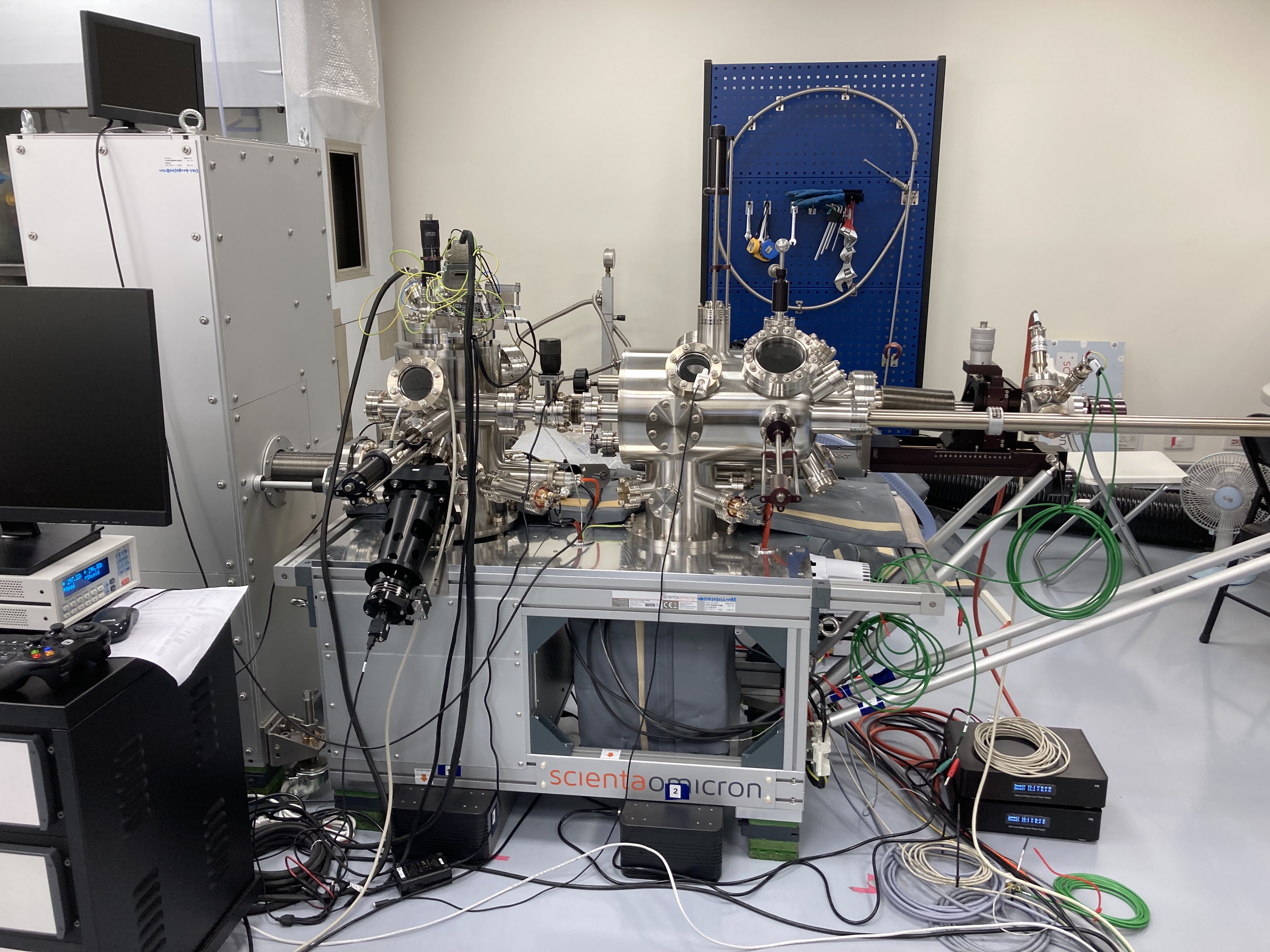
WELCOME TO OUR LAB
Exploring interfaces.
Understanding materials.
Our research lab is focusing on investigate the materials and device properties via scanning probe microscopy(SPM). By using cross-section scanning tunneling microscopy(X-STM), we can explore the interfaces behavior of heterostructure system. With light and electric modulation, we can do in-situ measurement of the electronic structure and relevent properties of the surface or interface of operating devices, which is important for future electronics and novel materials system.
We keep developing the key technologies for SPM to probe the facinating materials world in atomic scale in collaboration with multidisciplinary and international research group, and provide the key information to pave the way for future electrnoics.
FROM THE LAB
Latest news
- 恭賀 本實驗室研究成果 "Directly Probing the Carrier Transfer Length in 2D-Material Transistors" 刊登於SCI國際科學期刊 Nature (圖片資訊).
- 恭賀 本實驗室研究成果 "Electrostatically Tunable Moiré-Mediated Wigner States via Interfacial Potential Engineering in 2D van der Waals Heterostructures" 刊登於SCI國際科學期刊 Nature Communications
- 恭賀 本實驗室研究成果 "Direct Evidence of Coupling between Charge Density Wave and Kondo Lattice in Ferromagnet Fe5GeTe2" 刊登於SCI國際科學期刊 Nature Communications

